PAGE CONTENTS
Objectives
The objective of the WAKA project is to design, build, and test an Engineering Model of the RF line-up of a W to Ka-band frequency converter for future telecom payloads.
The targeted improvement is an enabling technology for future telecom systems based on the use of W-band for the gateway links.
In addition to the above objectives as per ESA-ITT, a low noise amplification section before the conversion mixer is designed and tested.
Therefore the unit under development is a full, standalone telecom receiver providing low noise amplification and down conversion to the Ka user band.
The project main tasks:
-
Identification of the technology/processes to be exploited for the design of the Down Converter.
-
Definition of the specifications and architecture, with reference to telecom programs of interest.
-
Identification, design and test of the critical building blocks and elements.
-
Design, manufacturing and test of elements of the RF line-up.
-
Design, manufacturing and test of the Down Converter.
Challenges
The project objective is to design a W to Ka-band frequency converter with Ka-band devoted to the user segment and W-band devoted to the gateway one, by using European state-of-art MMIC technology.
Such converter provides similar performances to current 30/20GHz and 50/20 GHz ones’, in order not to degrade the signal received by the user terminal.
While TAS-I can boast a considerable heritage in design and production of IF line-up in Ka-band, the main challenges refer to the development of the new elements operating in W-band, in particular on the design of several MMICs operating at W-band high frequencies.
System Architecture
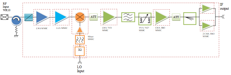
The complete block diagram of the W to Ka-band Receiver/Converter is presented in Figure 5.
The line-up is completed with the input WR12 isolator that guarantees input matching, the hermetic waveguide to microstrip transition and the IF line-up in Ka-band already available from heritage designs.
After the mixer, a 3dB pad is used to improve the matching of the mixer and keep at low level the intermodulation products.
A proprietary Ka-band low noise amplifier (LNA 7531) is used to increase the gain by 22dB followed by a microstrip filter that rejects the out-of-band intermodulation products and LO harmonics.
A Voltage Variable Attenuator(VVA) follows, which task is to compensate the gain variations with temperature. The VVA is driven by a DC network based on one thermistor and several Selected on Test resistors, implemented on a PCB located outside the RF hybrid module.
A further gain stage follows, i.e. the MMIC amplifier, providing 19dB gain. In order to adjust the in-band gain flatness, a suitable flatness equalizer MIC is employed. Good matching is ensured by its balanced configuration.
Finally, a balanced amplifier is used at the output to provide 18dB of linear gain.
Plan
The project is organised in seven main work packages:
WP 1000: Project Management
WP 1100: Baseline Specifications
WP 1200: Critical Elements Design
WP 1300: Critical Elements MFG & Test
WP 1400: RF line-up Design
WP 1500: RF Line up MFG & Test
WP 1600: Overall evaluation
The project milestones are:
-
Kick-off Meeting (KOM);
-
Preliminary Design Review (PDR);
-
Detailed Design Review (DDR);
-
Test Review Board (TRB);
-
Final Review (FR).
Current Status
The project has been concluded.
The results achieved are more than satisfactory:
-
The measured performances of the Receiver are well predicted by simulation and mostly in spec with the requirements.
-
The MMIC building blocks perform in good agreement with requirement.
-
The macro-hybrid module housing the Receiver includes a novel, low loss and hermetic waveguide-to-microstrip transition, which is compliant with the space environmental requirements.
Even though W-band is not deployed yet for satellite communication (gateway links), Thales Alenia Space Italia is committed in developing the basic building blocks of the RF sections of the payload, which include the W-band Receiver.