PAGE CONTENTS
Objectives
Future payloads for the next steps of SB NEO (2022/2025) will see their power further increased (>22kW), and an evolution of harness design is needed, using innovative solutions :
- to ease accommodation and integration
- to reduce mass and cost
These objectives can be reached by reducing the number of connection points and the cost per point.
This study is the first step : “definition phase”
The main objective of this phase is to perform a system study in order to define requirements, perform trade-off and specify a demonstrator (size and objectives, to be developed and built in a further phase).
The detailed objectives can be summarized as follow:
- Reduce harness mass (PCB Flexible)
- Reduce the number of wiring points (Smart connector)
- Reduce integration time (PCB Flex with Special Connectors)
- Reduce manufacturing time (PCB Flex
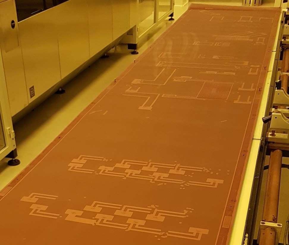
Flexible PCB by TRACKWISE
Challenges
Unlike a conventional wired harness, the Flexible PCB Harness is space-saving in height (less volume Z axis) but voluminous over its width.
In a SPB NEO cavity, the density of the elements (electrical and RF units, heat pipes, RF beams, RF waveguides, structural supports, etc.) is very high. It’s a real challenge to work on the layout of the future FLEX.
The main challenge of this project is to design a PCB that can be easily integrated around this equipment while respecting mechanical (PCB Flex fixing), electrical (double insulation, derating, voltage drop) and thermal (dissipation) constraints.
The second challenge concerns the Smart Connector, a compromise must be found between a high-performance, space-saving box with low dissipation and an attractive cost.
System Architecture
The product is a new harness architecture based on large flexible Printed Circuit Board, associated connectors, smart connectors embedding multiplexing and demultiplexing functions.
FLEX PCB design should be done in a co-operative and iterative manner with all other functions and subsystems to ensure enough space to route all electrical tracks to the unit connectors.
it will be necessary to evaluate the width of PCB FLEX PCB at each stage of 2D and 3D (CAD) design at the same time.
In other words, the 3D design must be completed in the same time as the 2D design.
In terms of length, the manufacturing process largely covers our needs. The total length of the panels deployed is about 3m.
The connectors are microD type, They can interface on a multilayer Flex PCB, these connectors are fitted with fast locking hardware.
The intelligent connector, which allows decentralization of the PLDIU, fulfils 2 functions : it is installed in a strategic location, at the input of each payload cavities, replacing the conventional interface connector support. It also provides a digital bus interface with the PLDIU and standard analog LVDS on the side of the payload cavity. This logic aims to reduce the mass of the harness thanks to decentralization.
Plan
The Kick Off of the study took place in March 2019.
The first step was to write the technical specifications of requirements, in parallel a Trade-off was carried out to highlight the gains in terms of mass and cost that can offer flexible PCB associated with smart connector.
These 2 documents were used as input for the following preliminary design phases.
These preliminary designs (Flexible PCB, PCB Connectors, Smart Connectors, CAD file) were written in parallel so as to be able to take into account the constraints of each one during all the study progress.
The study ends with the drafting of a System Implementation document which consider the implementation of technologies at the mechanical / layout, thermal and electrical levels and which proposes the Reference Architecture of the demonstrator (with alternatives).
Current Status
Today the preliminary designs of the different WP are delivered.